Two Bit MMU For the Z80
Eight bit processors can do a remarkable amount of work, but sometimes a 16 bit address space just isn't enough. We have had considerable success with a simple scheme that "bank switches" or "pages" a portion of system ROM. RAM is generally not banked, although there is no reason why this technique would not work for RAM as well as, or instead of, ROM.
This technique is also sometimes referred to as "mapped" memory, as it maps a large address space into a smaller address window. The terms "paged", "banked" and "mapped" are used more or less interchangably in this documentation.
It is interesting to note that the 68HC12 includes virtually the same circuit on-chip, through the use of the PPAGE register.
Consider a Z80 processor with 32K of RAM between 8000h and 0FFFFh (A15=1); and 32K of ROM address space from between 0000h and 7FFFh (A15=0). (That is, the product will ship with ROM, Flash, or EPROM. During development, this memory might be replaced by RAM for ease in debugging.) Let the 16K of ROM between 0000h and 3FFFh be always mapped. It contains the restart and interrupt vectors, the interrupt handlers, shared subroutines, and other "root" code. Let the 16K of ROM address space between 4000h and 7FFFh be mapped to one of eight pages, with the page number (high-order address lines) selected by a three bit latch somewhere in the processor's I/O or memory space.
Rules of use are the classic rules for overlays: The root can call subroutines in the root, or it can map to and call subroutines in the overlays. An overlay can call subroutines within itself, or in the root, but cannot call subroutines in other overlays. (If necessary, more complex software can be written to save overlay information on the stack and allow inter-overlay calls, but this is seldom necessary.)
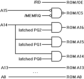
The hardware is pitifully simple: in addition to the 3 bit page latch, it requires 4 two input gates and a 128 Kbyte ROM.
Two Bit MMU For the Z80
As shown in the figure, when processor A15=1 or /MREQ=1 (/MREQ is the Z80's low true memory request), the ROM is deselected. When A15=0 and /MREQ=0, the ROM is selected, and one of eight 16K pages is accessed, depending on the values on ROM A16, ROM A15, and ROM A14. When processor A14=0, the outputs of the AND gates will be zero regardless of the value in the page latch (PG2, PG1, PG0). Thus, the root page is selected. When processor A15=0, /MREQ=0, and A14=1, the contents of the page latch is applied to ROM A16, ROM A15, and ROM A14, selecting one of eight pages. As page 000 is the root, there are effectively seven useful overlay pages.
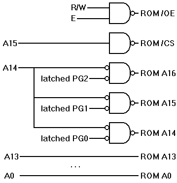
Two Bit MMU For the 68HC11
The second figure shows the circuit for ROM-at-the-top processors such as the 68HC11. Obviously, more or fewer latched page bits may be used with either processor to select more or fewer pages.
To change the memory page or bank, the processor must write to page latch. In many cases, especially if you use interrupts or multi-tasking, you will need to be able to save and restore the contents of the latch.
The simplest code is possible if the page latch can be read as well as written. Most microprocessor ports are read/write, and work well for this. However, these port pins often have other programmable functions and may be too valuable to be used for paging. If your memory banking logic is implemented in an FPGA or ASIC, it is usually easy to make the latch read/write. (If you aren't doing the hardware design yourself, it may help to bribe the hardware engineer with donuts.) The code looks like this (in pseudo assembly language for a microprocessor that distinguishes between memory and I/O space.)
| set page | save page | restore page |
|---|---|---|
    lda #PAGE5
    out pagelatch
|
    in pagelatch
    push a
|
    pop a
    out pagelatch
|
If you can't get a read/write page latch, the next best choice is a write-only latch all of whose bits are paging bits - none used for other purposes. In this case you will also need a RAM location to use as a readable image of the page latch. The software must follow the rule that any value to be written to the page latch must first be written to the image location. The code looks like this:
| set page | save page | restore page |
|---|---|---|
    lda #PAGE5
    sta pageimage
    out pagelatch
|
    lda pageimage
    push a
|
    pop a
    sta pageimage
    out pagelatch
|
Note that this code is safe to interrupts as long as every access to the page latch follows these rules and any interrupt routine that uses paged memory saves and restores the image and page latch. If an interrupt occurs between the sta and the out instructions, the image and the page latch will have different values. However, the interrupt will save the contents of the image. If the interrupt routine uses paged memory, it will write to both the image and the page latch. When the interrupt is complete, the interrupt code will restore the image, and then the page latch. Control returns to the interrupted code, which then (redundantly) writes to the page latch.
This scheme also works for task switches by a multi-tasking kernel. In this case, each task will keep its own desired page latch value. When a task switch occurs, the kernel saves the contents of the image to the suspended task's context, and the new task's page latch value is written to the image and to the page latch.
The worst choice is a port that mixes bits for paging with bits for other purposes, because the code must do a read-modify-write to merge the bits together. If you are using interrupts, your must disable interrupts during this read-modify-write sequence.
| set page | save page | restore page |
|---|---|---|
    disableints
    lda portimage
    and #MASK_TO_PRESERVE_OTHER_BITS
    or  #PAGE5
    sta pageimage
    out port
    enableints
|
    lda portimage
    push a
|
    pop a
    sta portimage
    out portreg
    (or do the bit merge if the other bits
    may have changed since you saved)
|
If you are using a compiler that supports banked or paged memory, the generated code takes care of the details of changing banks. If you are writing in assembler, you must do it yourself, perhaps following the same scheme.
Suppose that you write the C statement
stat = SomeFunctionInAnotherBank( "Ralph" );
This might generate assembly instructions similar to
    ldx #Ralph
    pshx
    jsr _BankSwitcher
    db 5
    dw $80AB
    std stat
Here we call a routine called _BankSwitcher to handle the banked call. The call is followed by a byte containing the page number of SomeFunctionInAnotherBank, followed by a word containing the address of SomeFunctionInAnotherBank in that bank. _BankSwitcher then
As described below, the db and dw embedded in the code stream can cause problems for NoICE, but a bit of care can avoid trouble.
Of course, if you are using the 68HC12, all of this is done in hardware and you simply use the CALL instruction to perform a banked call.
This discussion applies primarily to the classic serial monitor. BDM and other special communications methods may follow other rules.
The exact details will depend on your bank switching hardware. If you are using a RAM location as an image of the write-only page register, then the address of this location must be known to the NoICE monitor as well as to your user programs. This usually means that the image variable will be placed at an obvious location such as 0000 or 00FF etc.
Suppose that you decide to bank-switch the address range 0x8000 to 0xBFFF on a 68HC11. In MONHC11.ASM,
When NoICE sends a Get Status (FN_GET_STAT or 0xFF) message to the target monitor, the monitor can specify a range of addresses that should be banked. This is done in the informational string TSTG.
| Change this definition of TSTG without paging... |
|---|
;  Response string for GET TARGET STATUS request
;  Reply describes target:
TSTG    FCB     3                       ;2: PROCESSOR TYPE = 68HC11
        FCB     COMBUF_SIZE             ;3: SIZE OF COMMUNICATIONS BUFFER
        FCB     $80                     ;4: has CALL
        FDB     0                       ;5,6: BOTTOM OF PAGED MEM
        FDB     0                       ;7,8: TOP OF PAGED MEM
        FCB     B1-B0                   ;9 BREAKPOINT INSTR LENGTH
B0      SWI                             ;10+ BREKAPOINT INSTRUCTION
B1      FCC     '68HC11 monitor V2.0'   ;DESCRIPTION, ZERO
        FCB     0
        FCB     0                       ;page of CALL breakpoint
        FDB     B0                      ;address of CALL breakpoint in native order
TSTG_SIZE       EQU     *-TSTG          ;SIZE OF STRING
|
| ...to this definition of TSTG with paging. |
|---|
;  Response string for GET TARGET STATUS request
;  Reply describes target:
TSTG    FCB     3                       ;2: PROCESSOR TYPE = 68HC11
        FCB     COMBUF_SIZE             ;3: SIZE OF COMMUNICATIONS BUFFER
        FCB     $80                     ;4: has CALL
        FDB     $8000                   ;5,6: BOTTOM OF PAGED MEM
        FDB     $BFFF                   ;7,8: TOP OF PAGED MEM
        FCB     B1-B0                   ;9 BREAKPOINT INSTR LENGTH
B0      SWI                             ;10+ BREKAPOINT INSTRUCTION
B1      FCC     '68HC11 monitor V2.0'   ;DESCRIPTION, ZERO
        FCB     0
        FCB     0                       ;page of CALL breakpoint
        FDB     B0                      ;address of CALL breakpoint in native order
TSTG_SIZE       EQU     *-TSTG          ;SIZE OF STRING
|
When the target monitor starts up after reset, it must initialize the page latch, the RAM image, and the page register value (REG_PAGE) reported to the host.
| Change this initialization code without paging... |
|---|
;  Initialize memory paging variables and hardware (if any)
        STAA    REG_PAGE                ;NO PAGE YET
;;;     STAA    PAGEIMAGE               ;set RAM copy if PAGELATCH is write-only
;;;     STAA    PAGELATCH               ;set hardware page
|
| ... to this initialization code with paging. |
|---|
;  Initialize memory paging variables and hardware (if any)
        STAA    REG_PAGE                ;NO PAGE YET
        STAA    PAGEIMAGE               ;set RAM copy if PAGELATCH is write-only
        STAA    PAGELATCH               ;set hardware page
|
When the target enters the monitor at a breakpoint or unhandled interrupt, it must report the state of the page latch to the host as the page register value (REG_PAGE).
| Change this code in INT_ENTRY without paging... |
|---|
;  Save memory page
;;;     LDAA    PAGEIMAGE       ;GET CURRENT USER PAGE
        LDAA    #0              ;... OR ZERO IF UNPAGED TARGET
        STAA    REG_PAGE        ;SAVE USER'S PAGE
;
;  Return registers to master
        JMP     RETURN_REGS
|
| ... to this code in INT_ENTRY with paging. |
|---|
;  Save memory page
        LDAA    PAGEIMAGE       ;GET CURRENT USER PAGE
        STAA    REG_PAGE        ;SAVE USER'S PAGE
;
;  Return registers to master
        JMP     RETURN_REGS
|
When the host asks the monitor to read or write memory, it specifies a 16-bit address and an 8-bit page. The code for READ_MEM, WRITE_MEM, and SET_BYTES must set the page latch to the value sent from the host.
| Change this READ_MEM, WRITE_MEM, and SET_BYTES code without paging... |
|---|
; Set page ;;; LDAA 0,X ;get page/bank of memory address ;;; STAA PAGEIMAGE ;set RAM copy if PAGELATCH is write-only ;;; STAA PAGELATCH ;set hardware page |
| ... to this READ_MEM, WRITE_MEM, and SET_BYTES code with paging. |
|---|
;  Set page


        LDAA    0,X                     ;get page/bank of memory address
        STAA    PAGEIMAGE               ;set RAM copy if PAGELATCH is write-only
        STAA    PAGELATCH               ;set hardware page
|
When the host sends a RUN_TARGET (FN_RUN_TARG) command, the monitor must restore the page latch to the value of the page register (REG_PAGE).
| Change this RUN_TARGET code without paging... |
|---|
; Restore user's page ;;; LDAA REG_PAGE ;USER'S PAGE ;;; STAA PAGEIMAGE ;set RAM copy if PAGELATCH is write-only ;;; STAA PAGELATCH ;set hardware page |
| ... to this RUN_TARGET code with paging. |
|---|
;  Restore user's page
        LDAA    REG_PAGE                ;USER'S PAGE
        STAA    PAGEIMAGE               ;set RAM copy if PAGELATCH is write-only
        STAA    PAGELATCH               ;set hardware page
|
If the target monitor specifies that it uses paging, then NoICE will show addresses within the paged region as
xx:yyyy
where "xx" denotes the page, and "yyyy" denotes the address within that page.
For example, the address
12:8000
specifies address 8000 on page 12.
Page numbers are shown only for addresses in the paged range specified by the target monitor.
When entering an address in the paged region, the page may optionally be entered as a numeric value followed by a colon (:) when an address is specified. If no page is specified, then the current page as reported by the target and shown in the register window as PG will be used.
If you use a symbol name in an address expression, the page value (if any) given to the symbol when it was defined will be used. You can overridde a symbol's page value by preceding the symbol name with an explicit page number and colon. (You probably will never need to do this.)
If you use the LOAD command, you can specify the page in any of several ways:
Consider the bank-switching subroutine call described above:
    ldx #Ralph
    pshx
    jsr _BankSwitcher
    db 5
    dw $80AB
    std stat
Caveat 1: If you ask NoICE to disassemble this, NoICE cannot tell that the db and dw are data rather than instructions. Thus, it will disassemble them as best it can, possibly losing synch with the actual instruction stream. If you are using mixed source and assembly mode, NoICE will resynchronize at the next source line. Until then, however, things may look a bit odd.
Caveat 2: If you ask NoICE to "step over" the call you are likely to end up somewhere suprising. "Step over" works by inserting a temporary breakpoint after the jsr instruction - overwriting the db. If this were an instruction, there would be no problem: the breakpoint would be executed, NoICE would replace the original instruction, and all would be fine.
In this case, however, the subroutine _BankSwitcher looks at the contents of the byte after the jsr, and instead of seeing the "5" that ought to be there, it will see the breakpoint instruction. The value of this instruction is unlikely to be the page you want to go to, but that is where you are going to end up.
One way to avoid this is not to use "step over" on banked calls. You can step into and through the call, or manually set a breakpoint on the std.
Another solution is to use the CALLSKIP command to define that the subroutine _BankSwitcher is followed by three parameter bytes.
The basic NoICE 8051 monitor, mon8051.asm, assumes that your hardware combines the PSEN and RD lines, so that 8051 CODE and XDATA are combined into a single 64K address space. If you use this monitor, then you can easily add bank switching as above.
If you are using the monitor XMON8051.ASM, life is more complicated, because that monitor uses the "page" bits to specify an 8051 address space:
In this case, the monitor claims that the entire address range 0000 to FFFF is paged, so there is no place to put the bank/page. You could use a trick such as page addresses all above 10, to avoid clash with the "magic" pages shown, etc., but this is not likely to be pleasant. This is one case where a 8051-specific debugger is likely to be prettier than a mostly-generic debugger like NoICE.